How deep does the gallium damage go?
A 30 kV gallium beam leaves a damaged skin about 20–30 nm deep on every face it mills. Dropping to 5 kV cuts that to about 5 nm. At 2 kV it is about 3 nm. That is the whole reason the last polishing passes are done at low kV.
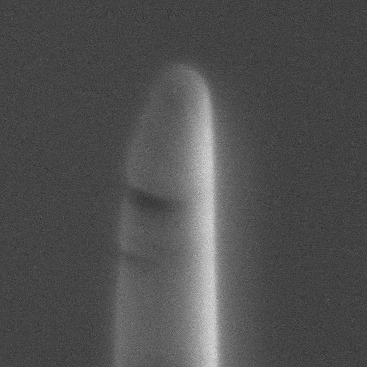
A needle I made in the FIB for atom probe, cropped to the tip (1:1, no zoom; the image is noisy because 2 kV imaging is gentle and dim). The tip is about 80 nm in radius, measured off this image. You cannot see the damaged skin in the SEM — it is a change inside the crystal, not a change in shape. The drawing on the right shows how thick that skin is, at exactly the same scale as this photo.
What is happening
A gallium ion is heavy and fast. When it hits the sample it does not stop at the surface. It bounces through the crystal, knocking atoms off their sites, and stops somewhere below the surface. The gallium atom stays there. The layer it travelled through is the damaged skin. In silicon it turns amorphous (the crystal order is gone). In metals it stays crystalline but is full of defects and gallium.
Higher kV = deeper skin. A 30 kV ion goes about ten times deeper than a 2 kV ion. So a face milled at 30 kV has a thick damaged skin, and a face polished at 2 kV has a thin one.
Why the low-kV pass works: the 2 kV beam mills away the deep 30 kV skin and leaves only its own shallow one behind. The damage is not repaired. It is cut off and replaced with less.
Why it matters for what you measure
- TEM foil: a foil has two milled faces. At 30 kV that is 20–30 nm of damage on each side. For a 50 nm foil there is nothing undamaged left in the middle. Tick the box above to see this drawn to scale.
- Atom probe needle: the skin is the first material the atom probe takes off the tip, so its gallium and its defects are what the first few million atoms of a run are made of.
- Micropillars and cantilevers: the skin is a hard, gallium-rich shell around a small volume. On a 1 µm pillar a 25 nm shell is 5% of the radius — and all of the surface, where cracks start.
The numbers, measured on silicon
| Beam energy | Damaged (amorphous) skin, each face | Source |
|---|---|---|
| 30 kV | 30.5 nm (this study); ≈22 nm is the most-quoted value; some report ≈10 nm | Huang et al.; Tescan; Sci. Rep. 2021 |
| 5 kV | 5.0 nm | Huang et al. |
| 2 kV | 3.1 nm | Huang et al. |
| 1 kV | 2.3 nm | Huang et al. |
| 0.5 kV | 1.5 nm | Huang et al. |
The spread at 30 kV is real: it depends on the angle the beam hits the face, the dose, and how the skin was measured. The low-kV numbers agree well across studies. Metals behave differently: they do not turn glassy, and the ions stop sooner in a heavier, denser metal — range estimates put 30 kV gallium at roughly 10 nm deep in copper, nickel or steel, versus about 27 nm in silicon or aluminium. What is left is a layer full of small defect clusters and dislocation loops. It can hold 10–20 at.% gallium. In aluminium, copper and nickel the gallium also forms compounds.
Practical rule used in most TEM-slice recipes: thin at 30 kV, then polish at 5 kV, then finish at 2 kV (or lower). Each step is done with a lower current too, so it removes less material and less of the sample heats up. The 2 kV finish is what makes atomic-resolution STEM possible on a FIB foil.
Sources. J. Huang, M. Löffler, W. Möller, E. Zschech, "Study of Ga ion induced amorphization in Si during FIB using TRIDYN simulation" (measured amorphous layer 1.5 / 2.3 / 3.1 / 5.0 / 30.5 nm at 0.5 / 1 / 2 / 5 / 30 kV); Tescan, "Argon vs Gallium for TEM lamella preparation" ("30 keV Ga⁺ milling can produce an amorphous layer approximately 22 nm thick on each side of the lamella"); Sci. Rep. 11, 21599 (2021) ("30 kV-FIB damages a lamella from its surface to a depth of the order of 10 nm"; 30 kV → 5 kV → 2 kV polishing sequence); J. Mayer, L. Giannuzzi, T. Kamino, J. Michael, "TEM sample preparation and FIB-induced damage," MRS Bulletin 32 (2007).
What are those vertical streaks (curtaining)?
The ion beam sweeps down the face. Anything at the top that mills slower or faster than its neighbours — a bump on the cap, a pore, a hard particle — casts a shadow that runs all the way down in the beam direction. That shadow is a streak. A smooth cap, a rocking stage, and a lower current all make the streaks fainter.
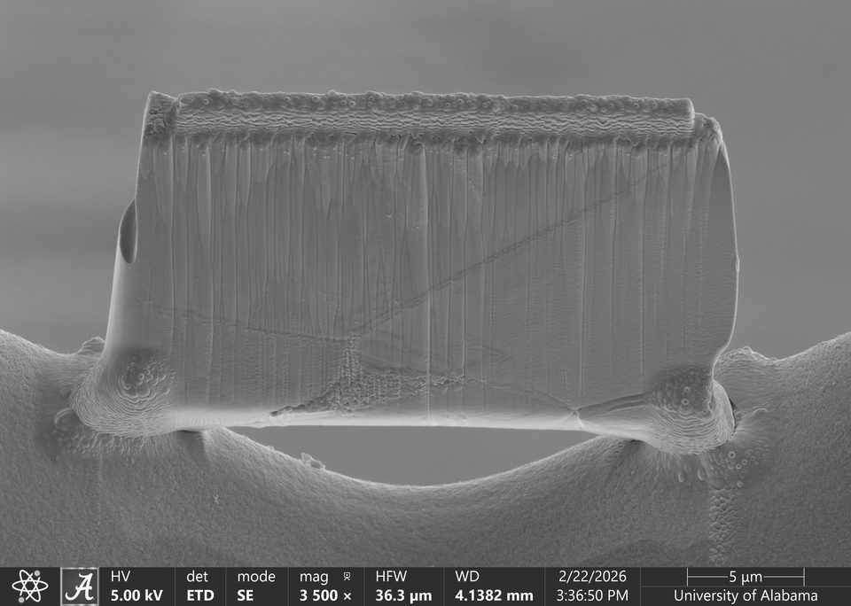
A lamella just after lift-out: welded to the copper grid, not yet thinned. The face is covered in fine vertical lines. They all start at the rough top of the Pt cap and run straight down. None of them run sideways. That is how you recognise curtaining: it always follows the beam direction.
What is happening
The ion beam comes from above and mills its way down the face. Now put a bump at the top of the face. The beam has to mill through the bump before it reaches the face below it. So the strip of face directly under the bump gets less beam than the strips on either side, and it is left standing higher. That higher strip then blocks the beam from the face below it in turn. The result is a ridge that runs down the full height of the face — one streak.
The same thing happens at anything that mills at a different speed from its surroundings: a pore (mills faster, makes a groove), a hard oxide or carbide (mills slower, makes a ridge), a grain boundary, or just roughness on the top surface. The photo above shows the most common case: the Pt cap itself is lumpy, and every lump starts a streak.
What makes it worse
- High beam current. A bigger beam removes more material per pass, so every difference in milling speed gets amplified.
- A rough or missing cap. Without a cap, the beam starts on the sample's own bare, rounded top edge — the worst possible starting line.
- A lumpy start. In the photo the streaks are strongest right under the cap and fade lower down, where the beam has had time to mill the ridges back. The worse the starting line, the further down they reach.
What actually fixes it
- A smooth, even protective cap (Pt or C) laid down before any milling. It gives the beam a flat starting line, and it keeps the real top edge of the sample from being rounded off.
- Rocking the stage a few degrees back and forth while milling. The shadow moves from side to side and gets averaged away instead of building up in one place. Rocking stages are sold for exactly this.
- Alternating the tilt between two angles (about ±2°) for the final passes does the same job without a special stage (a 2025 preprint measured this on TEM lamellae — linked below).
- Lower current for the last passes. Slower, but each pass removes less and leaves less behind.
- Thin the last bit from the other side, or from a clean edge, so the final surface was not milled through the rough cap at all.
Look at the "thinning" photo in section 03. The upper part of that lamella was polished at low current and is smooth. The bottom band was not, and still shows the streaks. Same slice, two treatments, side by side.
Sources. Tescan, Rocking Stage ("offsets curtaining caused by different sputtering rates, surface topography, and sample inhomogeneity"; lowering current alone slows milling 5–10×); Oxford Instruments, "The effects of Ga FIB milling on analysis" (curtaining from different milling rates; fixes: orientation, protective layer, lower current); "Reducing curtaining effects in FIB/SEM applications by a goniometer stage…" J. Vac. Sci. Technol. B 35 (2017); "Alternating angle milling suppresses streaking artifacts…" bioRxiv (2025) (the ±2° alternation); "Mitigating curtaining artifacts during Ga FIB TEM lamella preparation of a 14 nm FinFET device," Microsc. Microanal. (2017).
How do I know the lamella is thin enough?
You cannot measure the thickness while milling. You watch the electron image of the face change instead. As the foil gets thinner, the low-kV secondary-electron (SE) image gets brighter and smoother, and the backscattered-electron (BSE) signal gets darker, because electrons go straight through. A clean face also shows the crystal's grains — that tells you the damaged skin is gone, not how thick the foil is.
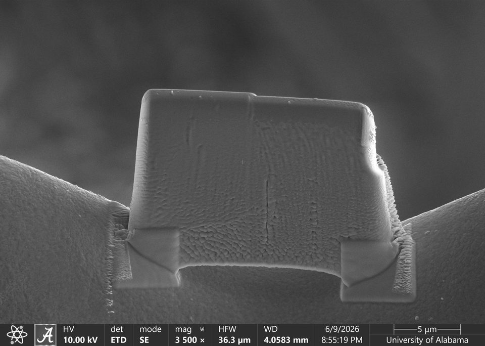
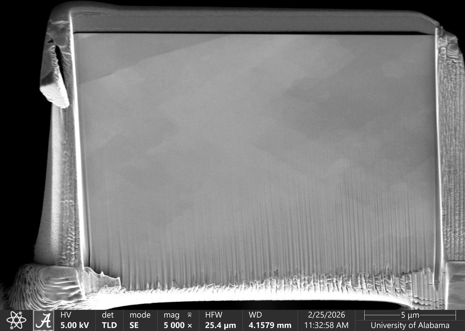
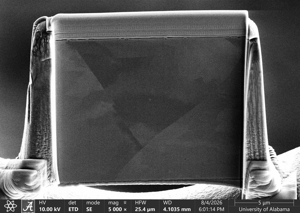
This one is copper, imaged at 10 kV before it went into the TEM. The face is not one flat grey any more: you can see grains and twin bands as different shades. Each grain has its atoms lined up in a different direction, so the beam gets in more easily in some grains than others, and they come out lighter or darker. This shows on a bulk surface too, as long as the surface is clean; a heavily damaged face hides it. So "I can see the grains" means the damaged skin is gone — a good sign about the surface, not a thickness measurement. The real check is still the TEM.
What is happening
The electron beam that makes the SEM image goes into the foil and spreads out. Some electrons bounce back out: backscattered electrons (BSE). Others knock loose slow electrons from the surface: secondary electrons (SE). The ETD and TLD detectors on this instrument mostly collect SE. Two things change as the foil gets thin:
- The SE image gets brighter. In a thick sample only the top surface gives off SE. Once the foil is thinner than the beam's reach, the back surface gives off SE too, and some get collected. The face looks brighter and more even. Edges glow brightest of all — electrons escape from both sides of an edge — which is why the bottom edge in stage 3 is a white line.
- The BSE signal gets weaker. Backscattered electrons come from a certain depth. When the foil is thinner than that depth, most electrons go out the back instead of coming back up. Below a certain thickness the BSE intensity drops in a straight line with thickness — which is why BSE, not SE, is what people use when they want a number.
The beam energy sets how deep the beam reaches, and so does the material. At 2 kV the beam gets about 30 nm into nickel or copper (about 100 nm into silicon); at 10 kV, about 0.4 µm (1.5 µm in silicon). So the kV you image at decides what "thin" looks like. Move the kV slider on the drawing and watch where the change starts.
Why it is a judgement call, not a number
The SE brightness depends on the material, the detector, and the contrast setting, so it is only a rough guide. One 2025 study says it plainly: SE brightness "lacks consistency" as a thickness signal, while BSE is linear with thickness below a limit. Most people thin by recipe, watch the SE image for the brightening and for the edge glow, and then confirm in the TEM.
A real recipe (two university facility procedures agree)
| Step | Ion beam | Until the foil is about |
|---|---|---|
| Rough thinning | 30 kV, 0.79 nA | 750 nm |
| Fine thinning | 30 kV, 0.43 nA | 300 nm |
| Final thinning | 30 kV, 0.23 nA (or 41–80 pA) | ≤150 nm, ideally 50–100 nm |
| Clean-up | 5 kV, 46–100 pA | removes the 30 kV skin (section 01) |
| Low-kV polish | 2 kV, ≈28 pA, 1–3 min (then 1 kV / 500 V if wanted) | removes the 5 kV skin; a few nm per side |
Both procedures also tilt the stage about 1.2–1.5° past 52° for each face, so the beam hits the face at a slight angle and the foil comes out even in thickness from top to bottom. The last 30 kV step can take the foil from about 300 nm to under 150 nm in one pass, so the operator checks the image between passes rather than during them.
What the three real photos show. Stage 1 is a freshly mounted lamella (nickel alloy, ~1–2 µm thick, dull and lumpy). Stage 2 is mid-thinning: the polished upper window is smooth and lighter than the bottom band. Stage 3 is near final: an even, bright face, with a glowing free edge. The thicknesses of these particular foils were not measured, so the photos are labelled by stage, not by nanometres.
Sources. ZEISS, "Reproducible TEM lamella thinning by FIB" ("With decreasing lamella thickness the SE yield from the lamella is enhanced, because of the contribution of those SEs emitted from its backside"; BSE intensity falls once the foil is thinner than the maximum backscatter depth); J. Uzuhashi et al., Microscopy (2025) ("the BSE intensity shows a simple linear relationship with the lamella thickness … below a certain thickness"; SE "lacks consistency"); CUNY ASRC, "TEM Lamella Sample Preparation" and Yale West Campus, "FIB manual TEM sample preparation SOP" (the recipe table); JEOL, SEM glossary: edge effect (why thin edges glow).
Why does the foil bend as it gets thin?
A foil is a sheet held along its top and sides, with a free bottom edge. Each milled face carries a damaged, gallium-rich skin that takes up more room than the crystal it replaced, so it pushes outward. A thick sheet is stiff enough to stay flat. A thin one bends, away from the face milled last, and the free edge moves most. If the foil is thinned while still joined to the block, the block holds it flat — and the final cut releases all that stress at once.
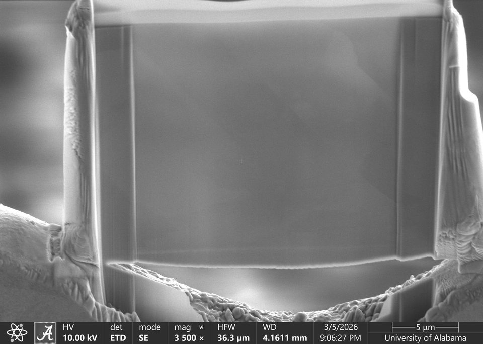
Same lamella as stage 3 in section 03. It sits on a grid post, so its bottom edge was cut free before thinning, with a straight milling pattern, when the slice was still 1–2 µm thick. Switch the overlay on. A dashed straight line joins the two ends of the bright bottom edge. The edge itself sits about 0.5 µm off that line (measured on this image; the field of view is 36.3 µm across). The picture is taken at 52°, which makes a bend out of the foil's plane look smaller than it is; the true bend is nearer 0.8 µm. A curve in the cut itself would look the same from one view, but the cut was straight, so bending is the likely reading. The top is held by the cap and the sides by thick walls. The free bottom edge is the part that moved.
What is happening
A sheet whose two faces are under different stress bends toward the side under less push. A FIB foil is in that state: the face the ion beam just milled carries a damaged skin (section 01) that takes up more room than the crystal it replaced. That skin pushes outward, so the foil bends away from that face. Milling the other face pushes back. The material can add its own locked-in stress from rolling, welding, or heat treatment.
Thinner = bends more. A sheet's stiffness scales with thickness cubed. Going from 200 nm to 100 nm makes it eight times easier to bend, while the skin pushing on it stays about the same. So a foil that looked flat at 500 nm starts to curve at 150 nm and can curl badly at 50 nm. The free bottom edge moves most; the welded top and thick sides hold still. The drawing above plays this out.
Cutting it free releases the stress at once. There are two ways to make a slice. In a lift-out (all the photos here) the slice is cut free first, welded to a grid, and thinned there; it bends slowly as it thins. In an "H-bar" the slice stays joined to the block along its bottom while it is thinned, and the block holds it flat. When the undercut then frees the edge, all the stored stress lets go together, and the foil can move while you watch. That is why the last cut is the risky one.
Why you see it in the electron image at 52°
At the 52° milling tilt the ion beam looks straight along the top edge of the foil and sees only a thin bright line (the ion-column image in section 03). The electron column, sitting 52° away, looks at the face. So the electron image is where the bend shows up: as a curved free edge, and as parts of the face going slightly out of focus.
What helps
- Leave a supporting frame. Thin only a window, and keep a thicker bar around it. If the geometry lets you thin before the undercut, do the release last, at low current, in small steps — not one fast cut.
- Cut stress-relief slots first. Two short slots near the ends let the stress relax in a small region instead of bending the whole span. This is standard in cryo-FIB ("micro-expansion joints") and works the same way on metals.
- Keep the thin window narrow. Tescan's practical limits for silicon: about 5 µm wide at 150 nm thick, 3.5 µm at 50 nm, 2 µm at 30 nm. Harder materials tolerate a bit more; softer ones less. A slice welded to the grid on one side only bends more than one welded on both sides.
- Low kV for the last passes, alternating faces. A thinner skin pushes less (section 01), and milling both faces equally balances the push.
- Don't touch it with the needle while the beam is on. A thin, warm, stressed foil is at its weakest.
Real practitioners on the same question (an Al lamella that "always bends"): gallium implanted
into one face adds volume there and bends the foil; the foil gets less stable as it gets thinner; an abrupt release at
the end is worse than a gradual one, so staircase milling and keeping both ends attached until the last step help.
— paraphrased from a ResearchGate practitioner thread, linked below
Sources. Tescan, "TEM lamella thickness vs width" (width limits; single-side-attached lamellae bend more); E. Holmström et al., "Atomic-scale effects behind structural instabilities in Si lamellae during ion beam thinning" ("the surface region is amorphized, which causes the region to expand and hence to bend the lamella"); Wolff et al., "Mind the gap: micro-expansion joints drastically decrease the bending of FIB-milled cryo-lamellae" and the follow-on "Mind the corner: fillets in cryo-FIB lamella preparation" (2025); ResearchGate: "Why is an Al lamella always bending when thinning it down in a FIB?". The drawing is a simple stressed-sheet picture (bend grows with the free length and with 1/thickness³); it is not a stress calculation for any particular material.
Why isn't the ion beam just a small dot?
The beam has a bright core a few nanometres to a few hundred nanometres wide, sitting on a faint tail that reaches many times further. The core does the milling you asked for. The tail damages the first micron or so outside the box you drew. Ions and electrons that scatter off the surface reach further still. The dark halo around every Pt strap shows how far that spill-over goes: mostly scatter, with the tail as its inner part.
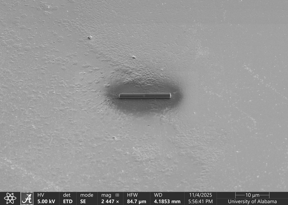
The only thing I asked the instrument to do here was fill one rectangle with Pt — the strap, about 15 µm long. It did. It also darkened an oval about 24 µm long and, after correcting for the 52° viewing angle, about 20 µm tall: 4–5 µm past each end of the strap and roughly 9 µm above and below it. That oval is thin, unwanted Pt and implanted gallium. Most of it comes from ions and secondary electrons scattered out of the beam spot, which break up the Pt gas wherever they land; the beam's own tail adds the part within the first micron or so. Any ion-beam imaging done while the gas was flowing adds to it too. Every strap has this halo. It matters when it overlaps the region you care about.
What is happening
A gallium ion beam comes from a liquid-metal source. The lenses focus most of the ions into a tight core, but not all of them: ions with slightly different energies, and ions that scatter inside the column, land in a wide, faint tail around the core. Measured beam shapes fit a "double Gaussian" — a narrow peak on top of a broad, low one.
The core is what the instrument quotes as "resolution": a few nanometres at the lowest currents at 30 kV. The tail carries a small share of the current, but it lands over a huge area, so its total effect is not small. One recent study measured a 30 kV, 7.5 pA beam in a TEM. The core was about 12–15 nm wide. The crystal was damaged out to about 500 nm from it at the dose they used — some forty times the core width.
Higher current = bigger core and bigger tail. The ion source always emits the same current. You choose the beam current with an aperture, a small hole in the column. A bigger hole lets through a wider cone of ions. A wider cone is harder to focus, for two reasons. The ions do not all have exactly the same energy (they push on each other as they leave the source), and the lens brings different energies to slightly different spots. And the outer rays of a wide cone always land a little further out than the inner ones. So the spot and the tail both grow. That is why rough milling is done at nanoamps and the last polish at tens of picoamps.
Where you meet the tail
- The halo around deposited straps (photo above) — mostly scattered ions and electrons, with the tail adding the innermost part. Keep straps clear of the region of interest, and switch the gas off before imaging.
- Rounding at the top edge of a trench, even under a cap.
- Damage next to a milled box extending well past the box edge — the 500 nm in the study above.
- Imaging with the ion beam. Every ion image is also a mill. A short look at high current still roughs up the surface around the field of view, and the tail reaches past it.
What the drawing shows
The curve is the beam's current density against distance from the beam centre. Both axes are logarithmic (each step is ×10), otherwise the tail would be too faint to see. The two labelled points are real measurements from the study named below (core ≈ 12 nm, damage out to ≈ 500 nm, at 30 kV and 7.5 pA). The slider is qualitative: it widens the core and the tail together as current goes up, following the direction every source agrees on, but the exact widths for a given current depend on the column and its alignment and are not calibrated for any specific instrument.
Practical habit. Assume anything within about a micron of a milled edge or a deposited strap has seen some beam. If that region is the one you will measure, mill a bigger box and clean up at low kV and low current, or move the strap.
Sources. Klingner, Hlawacek, Mazarov, Pilz, Meyer, Bischoff, "Imaging and milling resolution of light ion beams from helium ion microscopy and FIBs driven by liquid metal alloy ion sources," Beilstein J. Nanotechnol. 11, 1742 (2020) (beam profiles fit a double Gaussian, core + tail); Masteghin et al., "Quantifying the full damage profile of focused ion beams via 4D-STEM precession electron diffraction and PSNR metrics," Small Methods (2026) / arXiv:2511.00320 (30 kV, 7.5 pA, ~12 nm knife-edge resolution, disorder detected to ~500 nm); McClelland et al., "Bright focused ion beam sources based on laser-cooled atoms," Appl. Phys. Rev. 3, 011302 (2016) (chromatic and spherical aberration, Boersch energy-spread growth with current); "New directions in focused ion beam induced deposition…" (2025) (halo deposition from backscattered particles and proximity effects).